SCHEMATIC ENTRY
Basic Schematic Entry
Now that we know what we are building, we can get on with drawing it. We’ll start by familiarising ourselves with the basics of schematic design; picking components from the libraries, placing them on the schematic and wiring them together.
The design in question is relatively large and there is therefore a reasonable amount of drawing involved. We load a pre-supplied completed schematic when we reach the Design Verification section so, if you feel that you have mastered the basics at any point, there is no need to continue with drawing the remainder of the circuitry. We do however urge you to read through the full contents of the documentation as we introduce important features throughout.
The first thing we need to do is to get the parts from the libraries that we need in our schematic.
Selecting Parts from the Library
You can select parts from the library in one of two ways :
- Click on the P button at the top left of the Object Selector as shown below. There is also a keyboard shortcut for the Pick Parts command; by default this is the P key.

-
Right click the mouse on an empty area of the schematic and select Place – Component - From Libraries from the resulting context menu as shown below :

Either of these two methods will cause the Pick Devices dialogue form to appear.
For reference, the following is a list of all the components we will need for our design:
|
2N7002 |
24LC64 |
AVX0805NPO22P |
AVX0805X7R1N |
AVX0805X7R10N |
|
AVX0805X7R100N |
B82432T1103K000 |
BAS40 |
CHIPRES1K |
CHIPRES10K |
|
CHIPRES20K |
CHIPRES68K |
CHIPRES100K |
CHIPRES100R |
CHIPRES200K |
|
CONN-H2 |
CONN-SIL4 |
CONN-SIL6 |
CRYSTAL |
DSPIC33FJ12GP201 |
|
JUMPER |
LED-RED |
LM285-2V5 |
LM358 |
MAX1724 |
|
MPX4115 |
SHT15 |
TAWD106M025R0600 |
|
|
There are several ways in which we can find and import components from the libraries into the schematic. In the case of parts where you would know the part name its usually best to start the search with that. Try entering ’2N7002’ into the Keywords field on the Pick Devices dialogue form. This gives three components to choose from and we can then simply double click on the part in the results list to import it into the schematic. When you do this you should notice that the part now populates the Object Selector as in the following screenshot.
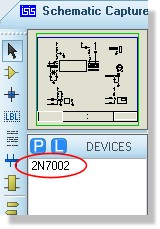
The 2N7002 in the Object Selector
Given that we know the names of all the parts we want we could simply proceed by using this technique to bring in all the components we need. However, this may not always be the case and Proteus provides several methods for finding parts in the component libraries. One of the most intuitive is to use the Pick Devices dialogue a little like an internet search engine, typing in descriptive keywords and then browsing the results to find a specific part. Try this now with the resistors, typing in ‘1k resistor’ in the keywords field to locate the CHIPRES1K component (double click on the part in the results list to import into the schematic). We could similarly search for ‘10k resistor’ to find and insert the CHIPRES10K component and so on.
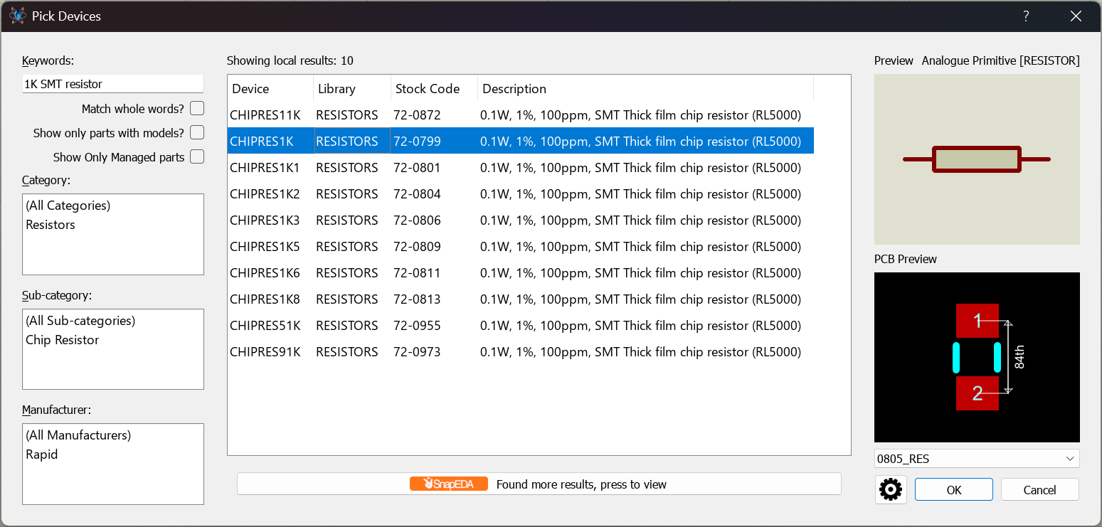
Picking a CHIPRES1K Resistor from the Pick Devices form / Websearch
Note that there are web search results accessible by clicking on the yellow bar at the bottom of the search display. This provides free access (you need to register a free account) to over 15 million library parts, meaning that if the part is not included with the installed libraries you can still source it from this dialogue form.
See Also:
You can customise the information displayed in the Pick Devices results list by right clicking the mouse on the results list. The context menu provides you with options to display Categories, Sub-Categories, Manufacturer and Library alongside each result.
It may be that we simply want to browse for a specific type of part and/or one available from a specific manufacturer. To take an example, clear out the contents of the keyword field and then select the Capacitors Category. In our design we are looking for some Nickel Barrier caps from AVX so we can further filter the results set by selecting Nickel Barrier from the sub-category field and AVX from the Manufacturer field. There are still a large number of caps available so we might type in ‘22p’, ‘1N’, etc. in the keywords field to isolate and select the particular components we require (AVX0805NPO22P, AVX0805X7R1N and so on).
Whilst this exercise is a little contrived given that we are starting from a preset list of parts, the techniques described are flexible enough to allow you to locate any library part quickly. Work through the full parts list for the design (as provided above) now using one or more of these methods to find and select the parts into your design. When you are finished you should have all of the required components in the Object Selector as shown in the following screenshot.
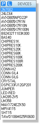
A Full list of required components
For example, if you wanted to search for a specific stockcode you would need to make sure that the stockcode column was enabled (right click on results list) and then type something like ‘digi <stockcode>’ to locate the digikey stockcode.
Similarly, if you want to search through only your own library parts, you can simple enable the library field and then type something like ‘user <partname>’; the user term will filter the results to the USERDVC library thus reducing the search range to your own libraries.
It is inevitable that at some point there will be parts needed for a project which aren't supplied in the installed libraries. In such cases you can quickly download and import the parts free of charge from popular third party vendors such as Ultra-Librarian, SnapEDA, Library Loader or PCB Library Expert. If the part cannot be found anywhere, and you have configured the AI assistant, ProPilot can build a library part for you from the datasheet. Both routes, along with drawing a part by hand, are covered in the Library Parts appendix to this tutorial; the import process is also discussed in detail in the reference manual and covered in video format on the website and our Youtube channel.
Placing Objects on the Schematic
Having selected the parts we need the next thing is to actually place them on the drawing area, the Editing Window, and wire them together. The screenshot below is the first sheet of the design we looked at in the Design Overview, and it is the target we are working towards in this section. Keep it to hand as a drawing guide; the split into logical blocks described in the overview is the order in which we shall tackle it.
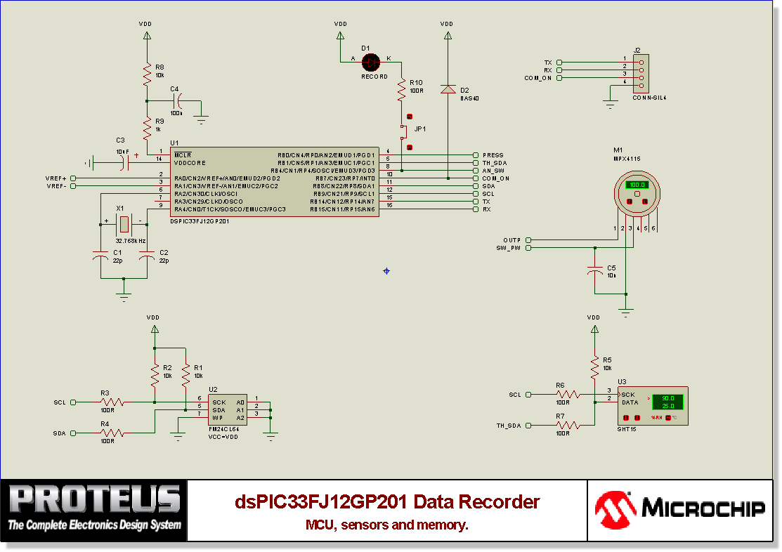
Main Sheet of the dsPIC33 Data Recorder Schematic
We are going to start off simply and complete the block of circuitry comprising the I2C Memory device as shown below.
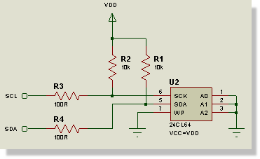
I2C circuit section
Begin by placing the I2C memory device as follows:
- Select the 24LC64 device from the Object Selector.
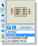
- Left click on the schematic to enter placement mode.
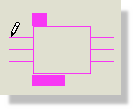
- Move the mouse to the desired location for the part, then left click the mouse again to ‘drop’ the part and commit placement.
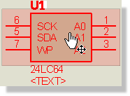
Often we need to move parts or blocks of circuitry after placement and now is a good time to cover the different ways in which we can do that. The procedure for this should be familiar to most users; we need to select the object(s) we want to move, left depress the mouse, drag to the new location and finally release the mouse to drop.
We can select an object in several ways as detailed below:
- Choose the Selection Icon and then left click on the object. This is a standard technique found in most graphical applications and will tag any object. Bear in mind when using this technique that you must change back to component mode for example, when you wish to perform other actions such as placing components etc.
- Right clicking the mouse on an object will both tag the object and present a context menu containing available actions on that object.
- Draw a tagbox around the object by depressing the left mouse button and dragging the mouse to form a box encompassing the object to be selected. This method will work for any object (or indeed sets of objects). Sizing handles are provided to allow you to resize the tagbox in the event that it does not fully enclose the object. This is the technique that should be used for moving multiple, connected objects or blocks of circuitry.
We’ll get plenty of practice moving things around as we lay out the schematic; for now just use one of these techniques to move the memory device down towards the bottom left of the Editing Window in roughly the same position as in the screenshot at the top of the section.
Having placed the memory device, we now need to get the peripheral circuitry down and oriented correctly. We are going to need two 10k pull up resistors and two 100 Ohm resistors for the data and clock lines. Additionally, we are going to need to use terminals to achieve connectivity with power, ground and other sections of circuitry. Begin by selecting the CHIPRES10K device and click left once on the anti-clockwise Rotation icon (shown below); note that the preview of the resistor in the Overview Window shows it rotated through 90°.
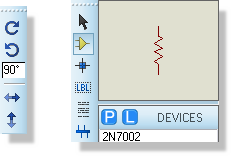
Using the Rotation Icons with the Overview window
Now place the resistor above and to the left of the memory device in the same way as before. Then, simply left click again on the Editing Window to start placing the second 10K resistor just beside the first one.
Next, select CHIPRES100R, rotate appropriately (see above) and place two to the left of the memory device in line with the SCK and SDA pins.
You can also rotate parts 'live' when in placement mode. Left click the mouse once to enter placement mode (at this point you will see the component outline following the mouse) and then use the '+' and '-' keys on the numeric keypad to rotate the component as you are placing it. Left click again to commit the placement in the normal way.
We use terminals in schematic design simply to terminate a wire and assign a connection. Often this connection is to either power or ground but it can just as easily be to another wire elsewhere on the circuit. Terminals allow us both to vastly reduce actual wiring (avoiding spaghetti schematics) and to make connections between different sheets on the schematic. To place terminals, start by selecting the terminal mode; this will switch the Object Selector and provide us with a listing of the available terminal types.
We need a power terminal, ground terminal and also two default terminals for the connections on the I2C bus. From this stage, placement and orientation are identical to any other object and should now be quite familiar. Place the appropriate terminals in their approximate locations now, such that the area around the memory device now looks something like the following
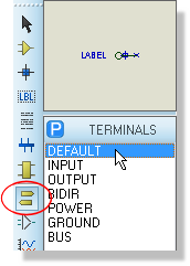
Selecting the Default Terminal
Unless you are fairly skillful, you are unlikely to have got all the components oriented and positioned entirely to your satisfaction at the first attempt, so now is a good time to practice moving things around as discussed earlier. In particular note that you can drag a tagbox around a group of objects to move the lot in one go.
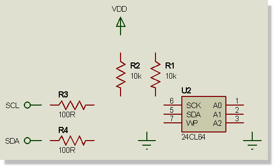
Components positioned correctly
Similarly, you can clear a selection (or group of selections) either by left clicking in empty space or by right clicking in empty space and choosing the Clear Selection option from the resulting context menu
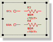
Dragging components
Remember that you can rotate while moving by using the '+' and '-' keys on the numeric keypad.
Grouping the Block
We have just dragged a tagbox around the block to move it as one, and that is a good moment to introduce object groups. A group is the persistent version of the tagbox. Instead of drawing the box again every time we want to shift the memory circuitry, we tell Proteus once that these objects belong together and it remembers.
Drag a tagbox around the whole block, taking in the memory device, the four resistors and the five terminals. Then right click inside the selection and choose Group Objects from the context menu. A confirmation message appears in the status bar naming the new group and the objects that went into it.
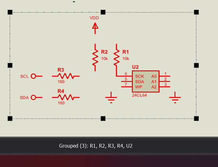
The I2C memory block selected and grouped, with the confirmation message in the status bar.
Now clear the selection and drag any single member of the block, the memory device for instance. The whole block moves with it. The important difference from a tagbox is that the group is saved with the design: come back to the project tomorrow and the block still moves as a unit. When you no longer want it, tag any member, right click and choose Ungroup Objects to dissolve the group again. The objects themselves are untouched.
Grouping now will not complicate the wiring we are about to do. Starting a wire from a pin is a placement operation rather than one of the group aware editing operations, so it behaves exactly as it would on ungrouped parts, and the wires you draw afterwards are not themselves members of the group.
Grouping does not get in the way of editing individual objects. Edit Properties always applies to the object you clicked on, so you can still rename a single terminal or change one resistor value without disturbing the rest of the group. If you left click a group member and do not move the mouse, the group expansion is cancelled and the Edit Properties dialogue opens for that object alone.
See Also:
Object Groups (Reference Manual)
Wiring Up
Having placed all the requisite components we now need to wire them together. There are three main techniques used to help make wiring a circuit as simple and quick as possible :
Modeless Wiring
There is no 'wiring mode' in the schematic editor - wires can be placed and edited at any time, without the hassle of entering a dedicated wiring mode prior to placement. This means less mouse travel, less mode switching and quicker development.
Follow-Me Wire Autorouting
After starting to place a wire, the proposed route of the wire will follow the movement of the mouse orthogonally to the termination point of the wire.
Live Cursor Display
The cursor will change as a visual indicator when wiring to show when a wire can be placed, when a wire can be terminated and when a wire is being placed.
The basic procedure for placing a wire between two pins is given below, using the connection between the SCK pin of the memory device and the 100Ohm resistor as an example:
- Move the mouse over the SCK pin on the memory device - the cursor will change to a green pen.
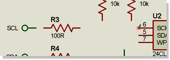
- Left click the mouse and then move it to the left until it is over the pin of the 100 Ohm resistor. The wire will follow the mouse and the cursor / pen is white during wiring
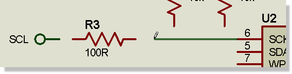
- Left click the mouse again to commit the connection and place the wire.
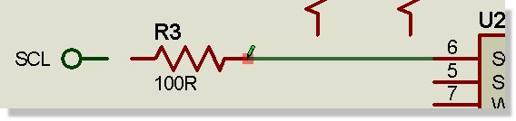
The procedure for wiring onto an existing wire is almost identical but there are a couple of items to note:
- You cannot directly start a connection from an arbitrary point on a wire; in our example you want to start the connections from the pin and terminate them on the wire.
- When you terminate the connection on another wire a junction dot will be placed automatically to complete the connection.
If, during a design, you want to make a wire-to-wire connection you must first place a junction dot on the wire and then wire from the junction dot to the other wire
If you want to adjust a wire after placement (for example, the wire from the SDA pin to the resistor) then simply right click on the segment you want to move and then either select the ‘Drag Wire’ context menu option or simply depress the left mouse button and drag to the new location.
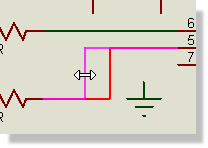
Dragging a wire
Armed with the above you should now be able to connect up all of the circuitry, so that your schematic now looks something like the following
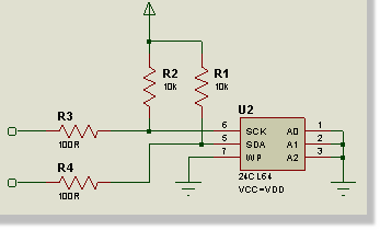
Schematic section with all parts / terminals placed
Remember, Proteus provides visual indicators to help you. If the cursor turns green you can start/stop wire placement.
See Also:
Connectivity by Touch
The following basic rules of thumb may be helpful:
- If you are placing the component you can attach to another component, wire or terminal directly.
- If you are dragging the component you can attach to another component pin, junction dot or terminal.
- If you are copy and pasting you can only attach it to a pin end, a bus pin, a junction dot or a terminal only.
Further information can be found here: Connectivity by Touch (Reference manual)
Making Connections with Terminals
The final thing we need to do to complete this block of circuitry is label the terminals. Terminal naming is extremely important as it denotes the connection to be made. We could name the terminals in any fashion we liked but sensible names make the schematic more legible and easy to understand.
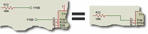
Terminal connection
Power, Ground and NC terminals are the exception to this rule, although there is no reason not to label them; an unlabelled power terminal is assigned to the VCC net and an unnamed ground terminal will be assigned to net GND. A pin connected to the NC terminal is NC and cannot then be connected on the layout.
Essentially what we are doing by labelling a terminal is making a connection to somewhere else on the schematic (a terminal with the same name) without placing a physical wire between the two objects.
As discussed previously the Proteus schematic is flexible enough to present you with several methods for editing parts - choose your preferred method for editing the terminal from the following:
- Double left click on the terminal.
- Right click on the terminal to select it and launch the context menu and then use the Edit Properties menu option.
- Enter Selection Mode, left click to highlight the terminal, then right click to launch it's context menu and use the Edit Properties menu option. Remember to exit selection mode when you are finished.
The block is grouped at this point, but that makes no difference here, since Edit Properties always acts on the single object you clicked on.
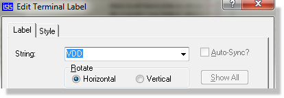
Having now launched the terminals dialogue form, type in VDD in the edit field as shown below and hit ok to exit the dialogue form
Note that, where appropriate you should always prefix numerical terminal values with a '+' or '-'. For example, a terminal labelled 12V is ambiguous and you should therefore ensure it is labelled +12V or –12V
Finish the job now by editing the other terminals and labelling them appropriately such that your completed circuit block now looks like the following:
Schematic section completed
See Also:
Power Connections
Proteus capture supports a powerful scheme for making power connections implicitly, thus vastly reducing the number of wires on the schematic. There are three main concepts involved that we will discuss in turn below.
Hidden Power Pins
Almost all relevant parts in the installed libraries have their power pins hidden (not visible on the schematic). The crucial point to remember is that in such cases is that by default the name of the pin denotes the net to which it will connect.
If you need all pins to be visible on the schematic (e.g. for auditing purposes) consider using the library import tool (Library menu > Import Parts) to bring in the parts you need. This process is quick and easy and works with library parts supplied from all major vendors.
See Also:
Hidden Power Pins (Reference Manual)
Power Rail Configuration
The easiest way to manage power nets and connectivity is through the Power Rail Configuration dialogue form, which is invoked with the Configure Power Rails command on the Design menu. If we do this now we can see that we have three pre-defined power supplies, namely GND, VCC/VDD and VEE. Changing the combo box at the top we should also see that the GND net is connected to the GND supply and that both the VCC and the VDD nets are connected to the VCC/VDD supply. It’s worth examining how this happened more closely:
- The GND net is created by connections to an unlabelled ground terminal.
- The VDD net is created by connections to the power terminal labelled VDD.
- The I2C memory has two hidden power pins, VCC and GND, which are assigned to nets bearing their names.
Managing power nets and power supplies is a very important concept so we’ll experiment a little to re-inforce the point. Exit the Power Rail Configuration dialogue form, right click on the I2C memory part and select Edit Properties from the resulting dialogue form. Next, click on the Hidden Pins button at the right hand side to view the hidden pins and their net assignments.
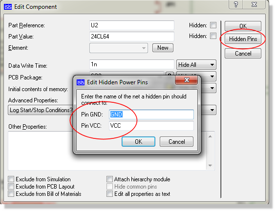
Hidden Power pins in schematic components.
Let’s change the power pin to be on net VDD, instead of the default of VCC. If we then exit the dialogue and re-invoke the Power Rail Configuration dialogue and switch to the VDD/VCC power supply we should see that the VCC net is no longer present (this was the only connection on our schematic so far).
While we are here and for completeness change the Voltage of the power supply to be 3.3V, which is actually what we will be using. In PCB Design this is useful only as a reference to ourselves but actually has significance in the software for simulation purposes.
This exercise, while useful in explaining how to view/change the power nets for individual components, had no effect on design connectivity. The software is clever enough to assign both the VCC and the VDD nets to the same supply and the Power Rail Configuration dialogue allows us to configure our power connectivity at design level.
Returning to the schematic now, edit the VDD terminal (right click, edit properties) and change the terminal label to ‘MY_POWER_NET’. If you go back to the Power Rail Configuration dialogue you should see that this is now an unconnected power net (a power net which is not associated with a power supply).
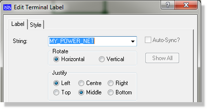
Changing the Terminal name
If we were doing this for real, we would now have to select the VCC/VDD power supply and then click the assign button to map our power net onto the correct supply.
If we had simply removed the label from the power terminal (instead of renaming it), it would have been designated to the VCC net and again everything would be done for us.
A final point worth noting is that new power supplies are created automatically when you label a terminal with a voltage. For example, labelling a power terminal +12V would create a +12V supply and assign the +12V net to the supply automatically. This means again that no action is required by the user.
In general usage therefore, the software will handle the assignments of power nets to power supplies and will create new supplies automatically. However, if you need more flexibility (for example, an analogue ground and a digital ground) then using terminal labels and the Power Rail Configuration dialogue gives you the control you need. Please see the reference manual for more information if required.
Let’s change our terminal label back to VDD for consistency before we move on.
See Also:
Power Rail Configuration (Reference Manual).
Global Power Nets
Power nets and connections are always global on a given sheet on the schematic. By default, they are also global to the design. However, if you do have a multi-sheet design and you want separate power supplies on different sheets you can isolate the supplies by un-checking the Global Power Nets box (Design Menu - Edit Design Properties dialogue form). This means that you need to explicitly wire through the sheets on the design but not within a given sheet. It is typically used only for the most complex of designs and is not relevant for the purposes of this tutorial.
Part Labels and Annotation
You should see that all the parts you have placed have both a unique reference and a value. A unique and sequential annotation is assigned to components as you place them on the schematic, although you can re-annotate manually if you need to.
You have full control over the position and visibility of part labels – you can change the values, move the position or hide information that you feel is unnecessary. The discussion below details how to manipulate part labels on a per component basis.
If you zoom in on any resistor you have placed you will see that Proteus has labelled it with a unique Reference (e.g ‘R1) and also with a Value (e.g. ‘10k’). You can edit both these fields and their visibility via the Edit Component dialogue form. Launch this dialogue form now by double clicking the left mouse button over the resistor (or using one of the alternative methods discussed previously).
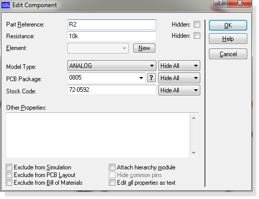
The Edit Component dialogue form
From the resulting dialogue form you can edit both the part name reference and, in this case, the resistance. Of more interest to us however, is the visibility options (highlighted in the above screenshot). It can be useful, particularly in densely populated schematics to hide some details displayed beside the parts – the trade off being that you would then need to edit the part as above to see it’s reference and value.
At this stage it is worthwhile familiarising yourself with editing components and hiding and showing references and values.
Some caution is required when changing part references in this manner. If, for example, you change ‘R1’ to be ‘R2’ then you will have two parts with the same reference on the schematic. This will cause netlist errors when working in the PCB module. If, however, you re-annotate using the new button on the edit component you are guaranteed a unique part reference.
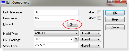
The 'New' button will automatically assign a new reference
Similarly, the Global Annotator (discussed later in the tutorial) will always avoid duplication of part references.
As well as the ability to hide part labels you can move them to a more convenient place. This is commonly used where you might want to place a wire over the current position of the label and need to free up some screen space. We will try this now with the 'R2' and the '10k' labels on the pull up resistor, moving them across to the other side of the component body.
Start by selecting the resistor. Now point at the label 'R2' and with the left button depressed, drag it to its new position to the left of the component body. Then do the same with the '10k’ label.
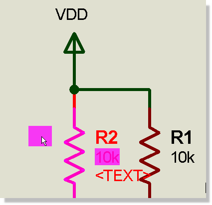
Dragging a reference
Timesaving Techniques & Block Editing
Armed with all of the basic techniques we can now look at the other blocks of circuitry on the front sheet of the design, practice what we have covered so far and introduce a couple of new timesaving techniques. Let’s start by drawing the dsPIC33 block as shown below:
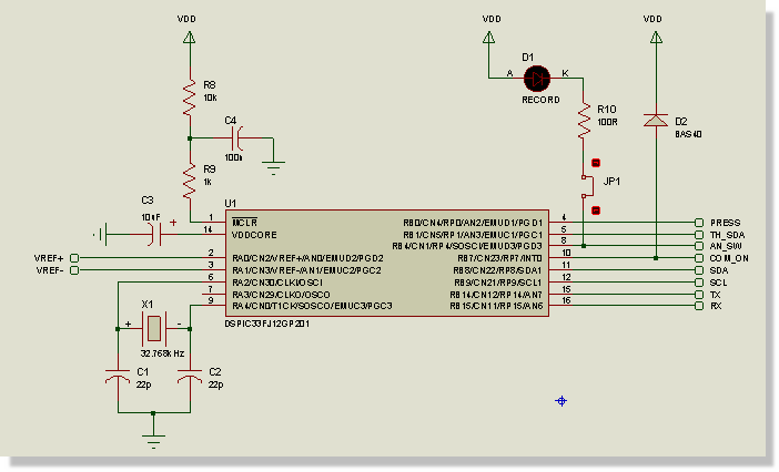
dsPIC33 Circuit section
You should be able to tell which components go where by comparing the component names in the Object Selector to the parts labels on the screenshot above. For clarity however, you can use the following table as a reference:
|
C1,C2 |
AVX0805NPO22P |
X1 |
CRYSTAL |
|
C3 |
TAWD106M025R0600 |
C4 |
AVX0805X7R100N |
|
R8 |
CHIPRES10K |
R9 |
CHIPRES1K |
|
R10 |
CHIPRES100R |
D1 |
LED-RED |
|
D2 |
BAS40 |
JP1 |
JUMPER |
|
U1 |
DSPIC33FJ12GP201 |
|
|
Begin by placing and wiring the oscillator and power sections (left hand side) of this circuitry using the methods outlined in the previous sections. When you are ready we’ll look at the right hand side, where we can use a couple of additional features to speed up the process.
The schematic editor provides a very useful feature to help with wiring when we are laying out a series of topologically identical wires. Essentially, it allows us to auto-repeat the last wire placed to form a new connection.
Start by rotating and placing a couple of the terminals to the right of the processor.
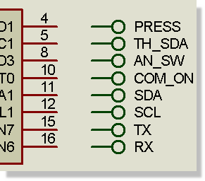
Terminals belonging to the dsPIC33
Now drag a box around the terminals and select the block copy command; this will allow you to quickly copy out three more sets of terminals ready for connection. Right click the mouse when you are finished to exit block copy mode
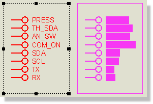
Block copying Terminals
Block copy is group aware. If the objects you copy belong to a group then the group structure is duplicated along with them, so the copy arrives as a group in its own right and is completely independent of the original. Moving one will not drag the other about.
Wire up the first connection from pin 4 (RB0) of the dsPIC to the terminal exactly as we discussed previously. Instead of repeating the process for the other seven connections simply hover the mouse over the next pin down (so that the cursor turns green) and double click. This will auto-repeat the previous connection, allowing you to rapidly wire up the other lines.
Note that this technique works by placing an identical wire to the one placed directly beforehand. It follows that the destination must be exactly the same distance away (i.e. aligned) and that you must perform the operations consecutively
We can now complete this section of circuitry, placing and wiring up the remaining components and labelling the terminals as per the screenshot at the top of the section. Note that a list of existing terminal label names is available as a drop down list from the Edit Terminal dialogue form (refer to the section on labelling terminals if you need a reminder).
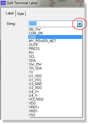
Drop down list of Terminals
It is highly recommended that you use this where applicable as it avoids the potential to make typing errors. Remember that terminal names denote connections so care should be taken during labelling.
With the processor block finished, group it as we did the I2C block: tag a box around it, right click and choose Group Objects.
You should be getting quite proficient at basic schematic entry now and the other three small blocks of circuitry on this sheet should present no problem. Group each of them as you finish it. When you are done your schematic should look something like the one below:
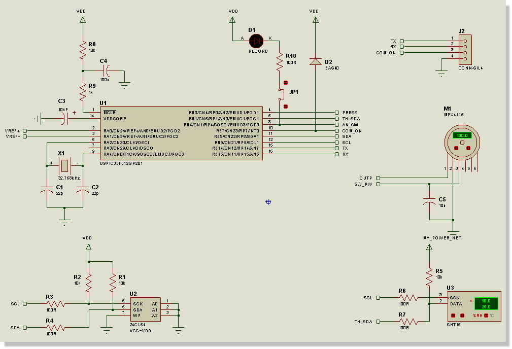
Completed dsPIC33 circuit
Comparing your drawing against a screenshot is not much of a check. If you have configured the AI assistant, this is a good point to get a second opinion: open the chat side bar with the ProPilot (AI Assistant) command on the Help menu and ask it to check for unconnected inputs or floating pins on this sheet. Phrase the request as an instruction rather than a question, because a question invites a yes or no answer and can give you a false pass. Component references in the reply are hyperlinked, so you can click straight through to anything it flags. Setting the assistant up and working with it are covered in Working with ProPilot in the reference manual.
If you feel comfortable with the topics we have covered to date, you can skip some of the drawing and load a pre-supplied completed schematic when we reach the Design Verification section.
Now that each block is a group, re-arranging the sheet is a matter of a few drags: pick up any member of a block and the whole thing travels with it, wiring included. The tagbox has not gone away and remains the right tool for an ad-hoc selection that does not correspond to a group, for instance a handful of objects spanning two blocks. Both work at any time, on any part of the drawing.
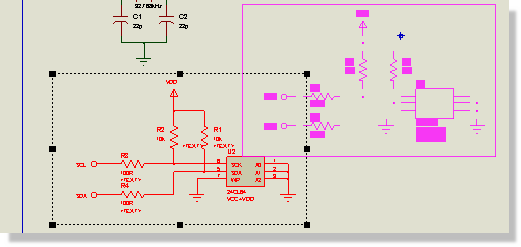
Moving a block of circuitry to the desired location